

CoolSNAP K4 Camera


Today’s thing is a Roper Scientific Photometrics CoolSNAP K4 Camera. The lineage of these cameras always confuses me, so this seems like a good opportunity to try and figure it out.
Roper Scientific has acquired a number of imaging companies.
Firstly, there was a company called Redlake Imaging. They made a number of cameras, in particular high speed 500fps+ cameras. Redlake Imaging was acquired by Roper Scientific in 1999. Roper also acquired part of Kodak’s imaging group at the same time. I’ve pulled apart Redlake ES/4 cameras, they use Kodak sensors.
Then there’s Photometrics which was founded in 1979 and released their first “CoolSNAP” cameras in 1999. Photometrics became a division of Roper Scientific at some point… but when exactly this happened is unclear. Finally, as of 2019 the whole thing has down been sold to Teledyne.
I suspect this camera owes more to Photometrics than Redlake as it seems to use the same LVDS (Cameralink-like) interface as all other Photometrics CoolSNAP cameras. But it does use a Kodak sensor…

Possibly the most interesting part of the camera is the sensor fixture itself. This is sealed module containing the sensor (which is bare die in a windowless package). The fixture contains a number of silica gel packs. This obviously helps sequester any moisture, and is particularly important in this camera as the sensor is cooled down to -25 degrees. If any moisture was present, condensation would be a problem…

It always amuses me that the Silica packs used here, embedded in the camera clearly indicate that they should not be eaten:

The sensor is thermally coupled using a metal block, to a stack of thermo-electric coolers (TECs). Typically TECs are stacked to help you get to lower temperatures. However, TECs are super-inefficient (typically ~10%). So when cooling, each stage needs to not only provide the required additional cooling, but also deal with all the heat produced by the poor efficiency of the next TEC stage.
For this reason, TECs in a stack tend to be increasingly large. And the CoolSNAP does indeed use a smaller TEC in the first stage, though the 2nd and 3rd stage TECs appear to be identical:

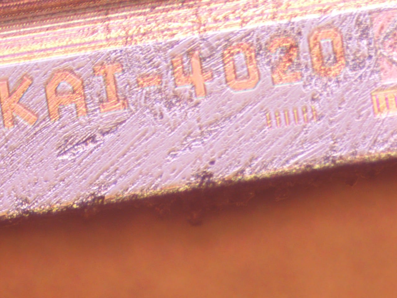
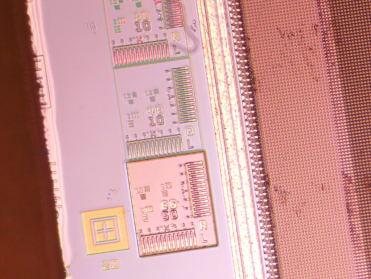
The sensor in this camera is a Kodak KAI-4020M. And it looks kind of pretty under a microscope:
The majority of the rest of the unit is taken up with a massive heatsink, pulling away all that heat produced by the TEC stack:

I’ll finish this post up with a few pictures of the PCBs. Over near the “data” connector is a DS90CR215, this is an LVDS driver supporting Channel-link. Channel-link is the physical interface used by Camera-link, an interface standard used by a number of Scientific cameras.
While Camera-link is a “standard” interface for the most part I’ve found it only works when a frame grabber card provides explicit support for a camera. The CoolSNAP K4 was generally provided with a PCI card (not shown here). Which I suspect is at least physically “Camera-link compatible”, but I don’t know of any other Camera-link cards this camera will work with.
Elsewhere on the board there are Sony CCD clock drivers and an AD9845 12bit CCD signal processor this integrates amplifiers and an ADC, seems like a neat part.
Surprisingly, I didn’t see an FPGA but rather a DSP, the DSP56309 this is a 100MHz 24 bit DSP, which must be doing all the signal processing and throwing the data out on the LVDS bus. There is a small Altera PLD however…
Aside from this, there’s nothing else I find particularly exciting on the boards, but further pictures are below!


Follow on Twitter. All content CC-by-SA.